A Technical Deep Dive on Elon Musk’s Neuralink in ~40 mins
Thorough Analysis of Neuralink’s Neural Implant System
Authors: Mikael Haji & Anush Mutyala
Neuralink is a groundbreaking Brain-Computer Interface company that strives to enhance the most intricate and sophisticated organ in nature — the human brain. Their team of immensely skilled individuals has created a sophisticated and cutting-edge brain-machine interface system with an incredibly high bandwidth, surpassing existing standards by a significant margin.

Table of Contents:
- Basic Overview of Neuralink’s SoC
→ Journey of a Neuron from Analog to Digital - A Deeper Look at the N1 Chip
→ Fundamental N1 Chip Pipeline
→ Data Packet Architectures - An Alternative Look at the N1 Chip
- Final Notes on Neuralink’s SoC
- Key Gaps with Neuralink’s N1 SoC
- Zooming Out: Applications For Neuralink’s Advanced Neural Interface System
- Zooming Out: BCI Readability | Plug-and-Play System
→ Challenge 1 | Firing Rate Variability
→ Challenge 2 | Latency Between Neural Signals & Cursor Movement - Zooming Out: Charging the N1 Chip
- Zooming Out: N1 Chip Testing
→ Firmware Testing
→ Implant Testing
→ Electrode Testing
→ Accelerated Lifetime Testing System
→ Gaps in N1 Testing - Zooming Out: N1’s Surgery Engineering
→ N1 Surgical Process of Implantation
→ Next Generation Development Process
→ Needle Design & Manufacturing
→ Proxy Design
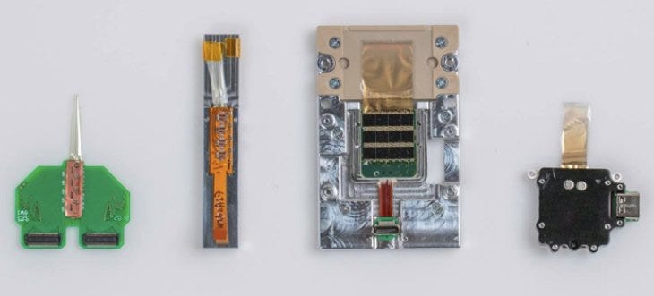
Co-founded by Elon Musk, Neuralink is building next-generation brain-machine interfaces with scalable neural channel density and real-time data processing unparalleled to anything in the BCI space.
With a typical chip life cycle (from Design → Verification → Tape Out) being approximately one to several years, Neuralink co-designs their chip with the rest of the system and the tight feedback loop has enabled their small team of analog and digital chip designers to get a record-breaking four tape-outs each year, all hyper optimizing major levers in the neural implant (including miniaturization, power consumption, reliability, economics etc.)
After many great conversations with people who have, and are working with Neuralink, we (Mikael Haji + Anush Mutyala) decided to spend the weekend breaking down the latest iteration of Neuralink’s N1 System on a Chip to come to a consensus on what’s going on at the:
Silicon Level of Elon Musk’s Human Brain-Machine Interface
Journey of a Neuron from Analog to Digital
There are 3 fundamental stepping stones in the Journey of a Neuron from Analog to Digital with their implanted technology from an electronics perspective.
1. Analog Processing of Neuron Spikes (Action Potentials)
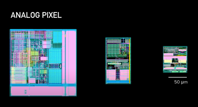
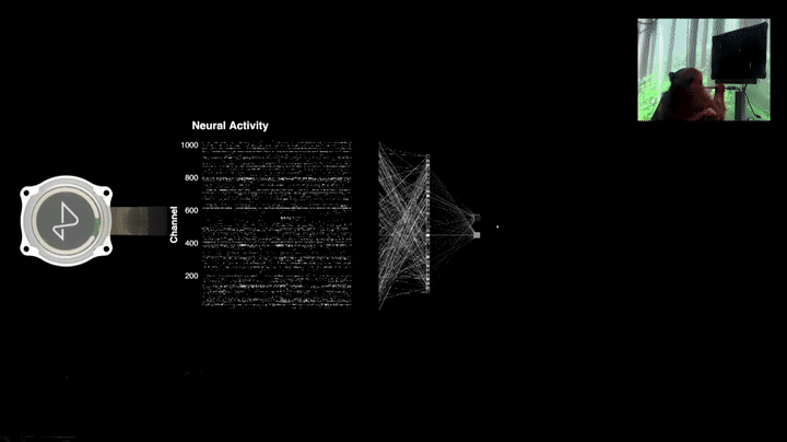
Before we convert analog neural signals into digital bits, we must begin by amplifying and filtering them. This is fundamentally the job of the “analog pixel.” As demonstrated in the figure above, an “analog pixel” simply comprises of the analog circuitry, filters, etc. The ideal scenario is one analog pixel per electrode so that we can configure them independently. As such, in the case of the N1 SoC, there are 3072 analog pixels and each one of these pixels takes up a significant portion of the physical space on the chip. Depending on how well these pixels work determines both the signal quality and the characteristics of the overall neural interface. When designing the analog pixel, there were three main considerations.
- Make it as small as possible so we can fit more
- As low power as possible so we can generate less heat and have longer battery runtimes
- As low noise as possible so we can get the best signals
The interesting part of designing the analog pixels is that the above considerations are at odds with each other. For example, we want to achieve lower noise on the amplifier so that more spikes can be detected, but as transistors get smaller, it becomes harder to get lower noise while keeping the power the same or less.
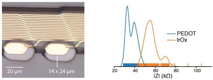
Another thing to note with this “stepping stone” is that amplitude is typically less than 10 microvolts. As such, when it comes to amplifying the signals, that would require a system gain of 43 dB to 60 dB in order to place the signals within the 10-bit resolution of the onboard ADC (~ 1 mV).
Impedance concerns compound the narrow ADC resolution because decreasing electrode geometries mean greater resistivity and noise in the system. In their paper published in August of 2019, Neuralink investigated two surface treatments (polystyrene sulfonate and iridium oxide), which have promising impedance characteristics.
2. Automatic Spike Detection
Once the signals are amplified, they are converted and digitized to 0s and 1s by our on-chip analog to digital-converter. Spikes or action potentials are often critical for certain BMI tasks. Currently, there are several methods for detecting spikes such as thresholding, PCA, etc.
One of the robust ways that Neuralink is going about detecting spikes is by directly characterizing the shape (different from template matching). In some cases, we can identify different neurons from the same electrode based on shape. Analog pixels can capture the entire neural signal samples at 20,000 samples per second with 10 bits of resolution resulting in over 200 megabits per second of neural data for each channel.
Neuralink is able to stream the entire broadband signal through a single USB C connector and cable. They wanted to eliminate cables and connectors so they modified their algorithms to fit the hardware by making it both scalable and low power.
Currently, they are able to implement the algorithm to compress neural data by more than 200 times and only takes 900 nanoseconds to compute, which is faster than the time it takes for the brain to realize it happened.
3. Every Channel Stimulation (Generation of Action Potentials)
The final stepping stone for Neuralink was electrode stimulation. They wanted the N1 SoC to provide electrode stimulation on top of reception. As of right now, the N1 chip can stimulate any one of its electrodes in groups of 64 — simultaneously. With an ability to stimulate even more neurons comes the performance of more complex tasks.
A Deeper Look at Neuralink’s N1 SoC
Based off Most Recent Patent Related to ASIC + Neuralink Launch Event + Neuralink 2019 Paper.
Moving on, we dive into the main patent relating to the ASIC chip that describes in detail the way that neural signals pass through the N1 module as well as the various customizations that can be made to the setup outlined in the white paper.
Chip Architecture & Fundamental Pipeline
As explained in the previous section, each N1 module carries multiple ASICs to maximize processing throughput. Several arrangements were proposed in the patent, most of which can be categorized either as:
- Linear
- Two-dimensional
For simplicity’s sake, the linear arrangement, where data is passed from one ASIC to the next, will be the focus of this review.
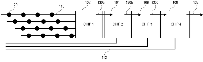
In this arrangement, the 1st ASIC receives data from its respective channels, packetizes the data, and pushes the processed signal in packets to the next ASIC in series. The 2nd ASIC then receives data from both the previous ASIC and its respective electrode and passes on newly packetized data alongside the packets from the previous ASIC to the next chip.
This process repeats until the aggregate data packets of all the chips are offloaded to another computing system from the last ASIC. The specific amount of data passed on to the next ASIC depends on what data management techniques are employed to improve power efficiency, which will be discussed later on.
Neuralink’s ASIC is composed of a few fundamental components:
- ports for inter-chip data transfer (left in, right out)
- array of analog pixels/neural amplifiers
- analog-to-digital converter (ADC)
- digital multiplexer
- controller
- configuration circuitry
- compression engine
- merge circuitry
- serialized/deserializer: act as inbound and outbound packet queues
The data flow within the ASIC begins with the analog pixels, which are tuneable amplifiers that are organized in an 8x8 grid. The ASIC imaged in the 2019 white paper boasted 4 of these amplifier grids, totalling 256 analog pixels for a 1:1 ratio with the number of channels interfacing with the chip. Low noise signal amplification is crucial for acquiring and conditioning weak neural signals that are collected by the electrodes. Additionally, the array of amplifiers may also take part in signal compression by applying thresholds set by the config circuitry on the raw data coming from the electrodes.
Once amplified, the signal is digitized by ADCs. In the setup described in the patent, there are 8 ADCs that receive signals from each of the eight rows of amplifiers. In the case of the version in the white paper, there would be 32 ADCs.
The digitized signal is then passed to the multiplexer, which serializes the data and filters for specific rows and columns from the amplifier array. The configuration circuitry, which can be programmed via a scan chain or JTAG interface (a method of injecting instructions into flash memory) to enable the desired mode, instructs the multiplexer on which analog pixels to sample from.
From a low-level perspective, the digital multiplexer works by implementing multiple NAND gates that control which input signals get passed on to the output. In a simple 2-input multiplexer, a separate control signal is sent to the multiplexer to switch between modes: either input 1 or input 2 passes to the output. The number of modes scales with 2^n where n is the number of control inputs.
The config circuitry is the main programming interface to the ASIC, that can switch the chip between several operating modes including skip channel, scheduled column, and event voltage spikes. These modes are essentially a set of instructions that implement thresholds in different components of the ASIC, including the compression engine, merge circuitry and multiplexer. A line in the patent summarizes the role of the config circuitry elegantly: “As the remaining circuitry are unique instruments in the orchestra playing specific roles, the config circuitry is the conductor.”
Program instructions are sent via a scan chain path to the config circuitry. Scan chains and boundary scans were originally created for testing integrated circuits without using physical probes. These scans work by utilizing test and scan cells to drive a signal onto a pin and across individual traces on a board. These cells are arranged like a shift register, where the initial scan-in input propagates throughout the circuit until the scan-out.
The config circuitry also sets all the parameters for the chip including the amp settings (# of amps to read out), polling frequency of electrodes, compression engine thresholds, etc. With stored program instructions, the config circuitry continues to send instructions to the rest of the chip during operation.
Continuing with the data flow, the serialized signal is sent to the controller which communicates with the compression engine and merge circuitry. The main function of the controller is to packetize data. The controller may orchestrate the analog-to-digital conversion by communicating which columns of the amplifier to sample from and when. The data packet architecture is illustrated in the next section. Additionally, the controller modulates the sampling rate or stop sampling from the amplifiers at chosen steps. Controller instructions can be altered every 6.25 µs (160 kHz).
From this point on, the data flow diverges depending on the modes programmed by the config circuitry. Data packets may first pass through the compression engine for compression or they may be sent straight to the merge circuitry. The compression engine performs the key function of effective data management when the array of amplifiers does not apply thresholds to the incoming data. In these scenarios, the compression engine receives the raw, high-bandwidth signals, which in some cases can be sampled at 20 kHz, from the amplifiers. Compression strategies predominantly involve applying thresholds to detect spikes in a specific range, summary statistics like channel-wise averages, and/or event-based triggers off-chip. Alternatively, information-theoretic lossless compression techniques like PNG, TIFF, or ZIP may be used. In some examples, the reduction in bandwidth from the compression engine can exceed 1,000 times fewer data.
These thresholds may be set on the voltage of the signal or the frequency of the signal. Low-frequency and high-frequency signals may not be valuable to the recorder and can be filtered out by the compression engine. Non-spike signals are discarded, essentially reducing the size of the data packets, and compressing the signal. For voltage-based thresholds, a technique called non-linear energy operator (NEO) may be used to automatically find a threshold that accurately detects spikes.
Briefly reviewing NEO, it essentially filters the signals for the periods at which there are fast frequency and amplitude changes of spikes, which can be seen as short peaks in the NEO filtered output.
NEO, represented by 𝝍[x(n)], of a signal x(n) can be computed as shown above. It simply compares the deviation between the signal at n time step and the signal at n-1 and n+1 time steps.
Furthermore, a threshold for NEO detection can be calculated as the mean of the NEO filtered output multiplied by a factor C. In this equation, N is the number of samples of the signal. C is found empirically and should be tested on several neural datasets beforehand to achieve the best results.
Both the compression engine and controller play a crucial role in throttling the amount of data being generated by each chip. Throttling allows for power and performance efficiency improvements for the N1 system.
Alternatively, during the Neuralink launch event, DJ Seo introduced a novel on-chip spike detection algorithm that involved directly characterizing the shape of a spike. This method is able to compress neural data by more than 200x and only takes 900 nanoseconds to compute, which is faster than the time it takes for the brain to realize it happened. This technique even allows for identifying different neurons from the same electrode based on shape.
Lastly, the merge circuitry receives data packets from the controller, compression engine, and the de-serializer. If you can recall, the de-serializer converts packets from off-chip links to on-chip, essentially queuing in the data from the previous ASIC. The merge circuitry essentially chooses which packets to send and when to do so from the data packets created on-chip and the ones from the previous ASIC. The chosen packets are then sent off-chip through a serializer.
Data Packet Architectures
Bandwidth is one of the primary limiting factors of a neural implant which calls for throttling and backpressure techniques to be implemented to prevent packet overflow. In regards to the maximum bandwidth on a single chip, it is as follows:
- For Analog Bandwidth, which is mainly driven by the signal characteristics of a neural spike is usually around 500Hz — 5 kHz. You want to double that to capture fine detail/timing of the signal and due to Nyquist Sampling Theorem, you need to sample at twice that frequency.
- For Digital Bandwidth, it’s basically the calculation of how many bits of data you’re processing per unit of time. The ASIC generates a 10-bit number per sample, which means that at 20 kHz, each channel is generating 200 kilobits of data per second (~200 megabits per second for 1000 channels).
Knowing this is vital as Neuralink’s processing stage needs to be capable of handling this volume of data, which guides a lot of the design decisions.
Backpressure is a concept programmed into the ASIC network by instructing the controller to stall packets being sent by the merge circuitry as packets are queued, in order to fill the available bandwidth. These packets awaiting passing are placed in buffers like a store and forward buffer. The system may also be able to gauge the extent of backpressure and can instruct the merge circuitry to drop back-logged packets at a certain predetermined threshold.
Strategies that can be employed to reduce dependency on backpressure have been outlined in the previous section, primarily involving thresholds to only record neurological events. These strategies avoid polling channels at 20,000 times per second, and instead only need to sample less than ten times per second in some cases. Also, due to the “recharge interval” of a neuron remaining relatively constant, built-in refractory periods can be integrated to pause recording for a set time.
When these strategies are used, data packets coming from each chip has a variable size vs. a fixed one that is relatively easy to predict when and how much data is being generated. Instead of opting for length standardization by using payloads full of null data sets, the structure of each data packet can be minimized for efficiency. Packets may be customized according to the needs of the data it encapsulates, minimizing empty packets and waster bandwidth, thereby relieving congestion.
In the figure above, an example packet structure is shown alongside a clock timer. The packet is composed of a header, the packet, and a trailer, which is the header for the next packet. The packet in this example is made up of a 10-bit word: 1 for the header, 8 for each row of amplifiers, and 1 for the trailer.
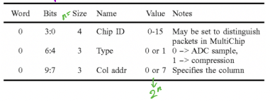
Above is an example header, with the size value determining the number of bits per category (Name), where 2^size is the range of values in the Value column. The header includes a chip id, representing the position of the ASIC in a network of chips.

In a scenario where data compression takes the form of voltage spike detection, a data packet may be organized as above. For example, the word “00001001” represents spike events occurring in rows 0 and 3. In a full bandwidth stream, packets are always 80 bits, 10 bits per row of raw data, and may not have a header. Also, column addresses are implicit in full bandwidth packets, as the columns stream out in the same order. In other packet arrangements, the number of words in the packet data depends on the system mode.
The packet above shows an alternative variable packet example where a command and receive signal is used for packet transfer and only 2 data words are present due to compression. The example signal sequence shown would control packet transfer between the various component parts of the chip including the controller, merge circuitry, etc. The request signal indicates a packet is being requested when the signal goes high. The receive signal indicates that the receiver is ready to receive a packet when it goes high. The request signal then indicates that the packet has been sent when the signal goes low. The receive signal indicates it is no longer ready to receive data when the signal goes low. Since the system can support more bandwidth than this specific chip is requesting, this means that the unused bandwidth can be allocated to other chips.
When determining which signals to pass on, in some examples, all rows in a column are read out every 160 kHz (8x faster than the high-bandwidth channel sample rate). For each column read, the controller would then build a packet based on information set in config circuitry. For example, if only 2 rows in a particular column are requested, the packet would consist of a header (10 bits) & the ADC data for those requested 2 rows (20 bits) for a 20 or 30-bit packet.
A 64-bit vector called SkipVec configures which of the 64 channels (8x8 amp array) are sampled/skipped. Channel n is skipped if the nth entry of SkipVec is set to 1 , i.e , SkipVec[n] = 1. For example, if column 1 is being processed by the controller, and SkipVec[15:8]=00110011, the resulting packet would be (assuming chip id 2 and ADC data = 0 for all rows):
If you recall from the table with the example header, the first 4 bits are allocated to the chip id and the last 3 bits are allocated to the column number. The proceeding words are the ADC data for the rows filtered for by the SkipVec. The packet does not inherently maintain information about the origin of row data, hence to interpret row data, the receiver must also know SkipVec.
When skipping columns, for each amp column read, the controller checks the particular time step (1 of 8 then repeats) and decides whether to send the entire column based on what the config circuitry instructs. When filtering columns, an 8x8 matrix called SkipCol may be used, where the col number and a time step are indexed from 0 to 7. In such examples, SkipCol may refer to the mathematical vector instruction for the amplifier to pass event data. Let t be an integer representing absolute time, and k = % 8. Then we skip column n at step k if SkipCol [ n , k ] = 1.
For example , if SkipCol [7 : 0,3 ] = 11001100, this corresponds to columns 0, 1, 3, and 4 being sent on time steps 3, 11, 19, etc. These same columns might also be sent on other time steps as well.
When filtering by columns, it is generally more efficient to send the entire column in a packets vs. sending subsets of a column due to header word overhead.
Lastly, for packet management across the series of ASIC chips, traffic control is necessary to ensure sufficient amounts of information from each chip exit to off-chip systems. If each chip merely passed on all packets as they were received, the data flow off the chipset to the computer for storage and processing may be biased toward the closest chip, especially in a 50–50 arrangement (the next receives half of the packets from the incoming channels and half from previous chips).

In the case of a 50:50 arrangement with full bandwidth (refer to abbreviations from FIG.1b, C(n) represents the chip id):
- D1 w/ 100% weightage → C2, all of the packets from chip 1 transfer to chip 2
- [D1, D2] w/ 50% → C3
- [D1, D2] w/ 25% + D3 w/ 50% → C4, etc.
As you can see, as more packet transfer steps are added, the data from the prior packages drop by a factor of 2, creating an unfair bias for the last chip.
Several solutions are proposed for this problem, including offsetting the bias at each transfer step. For example, when chip 2 passes packets to chip 3, the number of packets from chip 3 are not passed with 50% of the bandwidth, rather they are passed with 33% of the bandwidth and those from the first and second chip are passed with 66% of the bandwidth. The fourth chip would only use 25%, biasing the previous chips to also share 75% in 25% splits.
Individual merge circuitry components in each chip may be programmed with these metering instructions to create balanced data packet scenarios. In some examples, the buffers in the serializer and/or deserializer may also be instructed to aid the merge circuitry in this balancing act or meter the packets it is passing along as well.
Alternative Look at Neuralink’s N1 SoC
Based of Submission to 2021 Symposium on VLSI Circuits + 2022 Show & Tell.
In 2021, the Neuralink team submitted a 1024-Channel Simultaneous Recording Neural SoC with Stimulation and Real-Time Spike Detection architecture. While there are some similarities to the initial design, Neuralink has also made significant advancements. It’s worth noting that the details of the SoC architecture in this update are the most recent, but it’s probable that Neuralink has made further enhancements.
This paper introduces a neural system-on-chip (SoC) that is only 5x4mm² and designed for clinical applications, which means it needs to be small and power-efficient. The SoC can record and stimulate from 1024 implanted electrodes through a serial digital link (similar to previous design), and it includes configurable spike detection that can greatly reduce off-chip bandwidth.
The design also has integrated power management circuitry with power-on-reset and brown-out detection, resulting in a total power consumption of just 24.7mW. This makes it the lowest-power and highest-density AC-coupled neural SoC that can record both local field potential (LFP) and action potential (AP) with a bandwidth of 5Hz-10kHz.
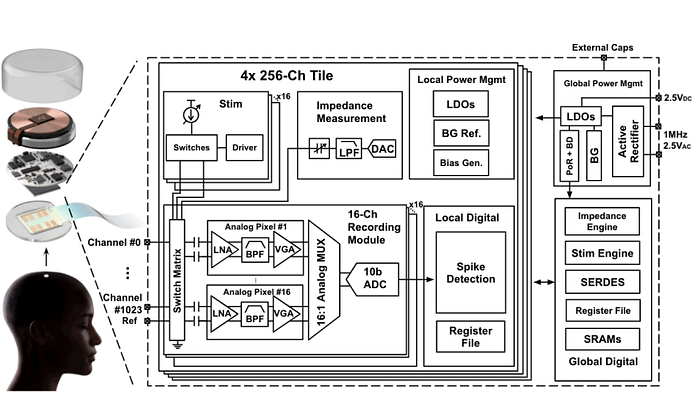
Fabricated in a 65nm CMOS process, the system-on-chip (SoC) architecture can be illustrated through the block diagram above, which showcases its impressive components. The SoC is comprised of:
- Four 256-channel tiles, each of which contains 256 neural amplifiers
- 16 successive approximation register analog-to-digital converters (SAR ADCs)
- 16-core stimulation engine with each core linked to 16 channels
- An impedance measurement engine
- A local power management module
- A digital signal processor with integrated spike detection
The input switch matrix of the SoC allows for dynamic configuration of channel mode, which can be set to record, stimulate, or measure impedance. Additionally, the reference connection can be adjusted based on the experimental setup, whether it be to a reference electrode, a nearby electrode, or the system ground.
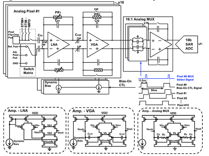
The detailed circuit diagram of the module, as depicted above showcases the intricate setup of this state-of-the-art technology. The analog pixel within the module is composed of capacitive-feedback operational amplifiers (OPAMPs), which serve as low-noise amplifiers (LNA) and variable gain amplifiers (VGA). These components work in harmony to amplify and configure LFP and AP bands with configurable gain.
To ensure that the LNA input transistors are working within the correct DC bias operation region, input AC-coupling capacitors are used to block unknown DC offset from the electrodes in the brain. The pseudo-resistor (PR) in the feedback path plays a critical role in setting the high-pass filter (HPF) cutoff frequency and DC input bias of the pixel. With the tunable PRs, the HPF cutoff frequency for LFP and AP bands can be adjusted accordingly.
Each analog pixel within the module has its own flip-chip bonding pad, which is connected to the positive input of the LNA. To implement an area-efficient anti-aliasing low-pass filter (LPF), a two-stage Miller compensation architecture is chosen for the VGA. The output of the VGA is then multiplexed onto a 10-bit SAR ADC with a switched-capacitor amplifier based 16:1 MUX, providing sufficient drive capabilities to fully settle the ADC within the sampling window.
To ensure the efficiency of the module, a dynamic bias circuitry is employed. This circuitry turns off the LNA and VGA right after the output is sampled, resulting in the consumption of only 25% of the static power. With the settling time of the analog pixel output from an unpowered state to sampling being much shorter than the channel sampling period, the overall analog pixel dimension is kept small, measuring 65×71µm2, including routing channels, input switch matrix, dynamic biasing, and a flip-chip bonding pad.
In the global power management of the module, the first stage of the cascaded LDOs takes 2.5V DC or an active rectifier output generated from 1MHz 2.5V AC. The second stage LDOs generate separate power rails for the local power managements, stimulation engines, pad drivers, and digital to reduce noise coupling between power domains. Each 256-channel tile has its own local power management to distribute power evenly through the entire tile.
The module boasts a 64-core stimulation engine, which is capable of stimulating all 1024 channels with arbitrary shape current waveform in any combination of electrodes in a 16-channel recording module. This means that researchers and scientists can study brain activity in unparalleled detail, allowing for new insights and discoveries.

Above, we see an overview of the impressive capabilities of the stimulation engine in the 256-channel tile. The system uses a single current source to ensure charge balance during stimulation, minimizing damage to both the electrodes and the surrounding tissue. With 16 stimulation engine cores, the system is capable of outputting up to 600µA with a compliance voltage of +/- 1.8V and 8-bit tunability. This level of control allows for the generation of waveforms with a time resolution of 7.8125µs, and programming of various stimulation parameters such as current amplitude, pulse duration, inter-pulse gaps, and frequencies via a serial digital link.
The impedance engine, which is responsible for testing the impedance of each channel, has a CORDIC function generator that generates the impedance test signal according to the configuration set in the registers through an RDAC and a 2nd-order analog LPF with a 10kHz cutoff frequency. The engine can be programmed to test any channel in the tile.
To handle the enormous amount of data generated by the system, the 64 320kS/s 10-bit ADCs produce a total output data rate of 204.8Mbps. In order to make the system more scalable to handle even more channels and to reduce power consumption from the SERDES, the architecture includes an on-chip spike detection algorithm. This algorithm is configurable and real-time, allowing it to detect spikes and reduce the data rate by an impressive 1250x. This feature is especially useful for BMI decode algorithms that use spikes as inputs.
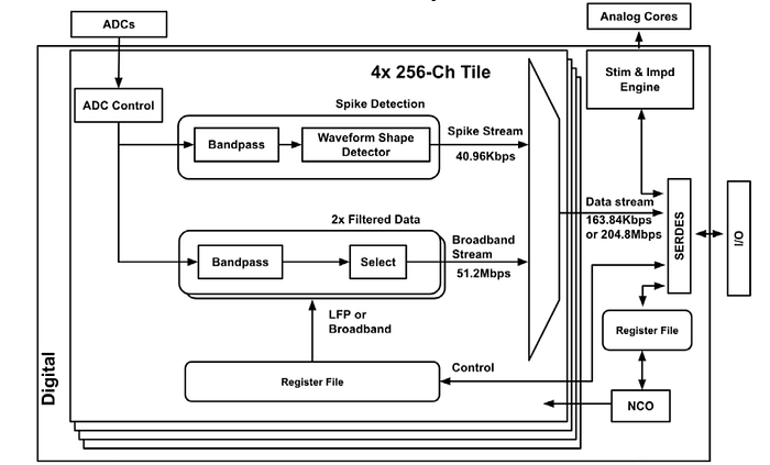
The digital block diagram, as illustrated above, is a key component of the system. Upon digitization by the ADC, the samples are divided into three separate datapaths, each with its own unique purpose. One path is dedicated to spike detection, while the other two are reserved for debugging and LFP modes, respectively. Each path contains a programmable 2nd-order IIR filter to process the data.
In the spike detection path, the system estimates the shape of the waveform and filters out samples that do not meet the pre-specified criteria. The other two paths allow the user to send raw and filtered data for a selected subset of channels, as desired. Finally, all three streams are merged and sent to the SERDES for transmission.
To achieve optimal performance, the digital block diagram is implemented using fixed-point arithmetic with custom precision, avoiding costly floating-point operations. Number representation throughout the pipeline is also optimized to minimize misclassification, achieving a remarkable >99.7% match to floating-point computation. Overall, the digital block diagram plays a critical role in the system’s success by enabling effective processing of the data and facilitating the communication of the results.
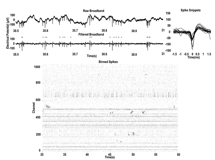
The snapshot above provides a visual representation of the output obtained from the implanted device in a pig. The figure depicts raw and filtered broadband signals, spike snippets, and 1024-channel binned spikes. These signals provide important information about the neural activity in the pig’s brain, which can be used to study brain function and develop new treatments for neurological disorders. The raw and filtered broadband signals capture the overall activity in the brain, while the spike snippets show the precise timing and shape of individual action potentials. Finally, the 1024-channel binned spikes illustrate the distribution of neural activity across the different channels of the device.
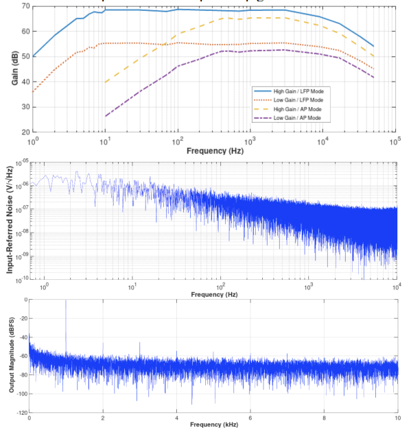
The recording module’s performance can be analyzed through various measurements, such as frequency response, input-referred noise, and output spectrum, all of which are displayed above.
- Input-Referred Noise → The LFP and AP modes produce a noise of 6.8µVrms (5Hz to 1kHz) and 8.98µVrms (300Hz to 10kHz), respectively.
- THD → THD is a crucial aspect to consider when evaluating the module’s performance. With a -0.79dBFS input, the THD measures at 0.57%.
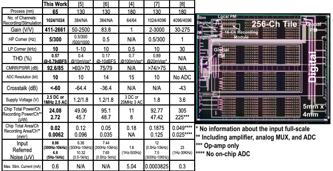
Above is a concise summary of Neuralink’s work’s measured performance, providing a comparative analysis against the integrated AC-coupled neural recording systems for both LFP and AP. The achieved Common-Mode Rejection Ratio (CMRR) and Power Supply Rejection Ratio (PSRR) are an impressive 92.6dB and 85dB, respectively. Notably, Neuralink has achieved exceptional crosstalk suppression, with an adjacent channel crosstalk of less than -60dB.
Their System-on-a-Chip is highly efficient, consuming a mere 24.7mW in a typical configuration, inclusive of all power management circuits, digital, clock, and I/O drivers. The excellent power efficiency of their SoC is matched by its compact size, with a mere 0.02mm² chip total area per channel, setting a new benchmark for integration density.
In addition to the impressive CMRR, PSRR, and crosstalk suppression, their work boasts the lowest recording module power consumption per channel of 2.72µW, making it an ideal solution for long-term implantable systems.
Overall, Neuralink’s work represents a significant advance in the field of neural recording systems, providing unparalleled performance metrics in a compact, efficient package.
Final Notes on SoC
By leveraging the features of Neuralink’s system that have been described above, there are many levels of customization and reprogrammability that can be used for the purpose of the user.
For example, if you want to get a snapshot of a calibration curve for spike detection, you could allow titration of high fidelity information with compressed data by sampling different sets of amplifiers at different times. Chip parameters may be configured on-the-fly to help visualize the effects of different parameters from the user’s perspective in real-time.
Furthermore, an important detail that Neuralink raises is that the systems outlined in the patent for their ASICs can also be modelled/replicated using software, processing components, hardware logic circuitry, etc.
- A general-purpose computer could be used to run the multi-chip system
- Field programmable logic arrays, which is a configurable integrated circuit programmed with special-purpose instructions can also be used to implement the modules described in the patent
- For the analog pixels/amplifiers, a variety of component types can be used for the device technology, metal-oxide-semiconductor field-effect transistor (MOSFET), complementary metal-oxide-semiconductor (CMOS), polymer technologies, etc.
Key Gaps with Neuralink’s N1 SoC
Several recurring technological gaps are addressed throughout the patent and in other Neuralink sources at large.
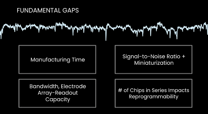
The technological gaps with the N1 SoC can be summarized as follows:
- Signal-to-noise ratio from the amplifier scales with the size of the transistors, but as transistors get smaller, it becomes harder to get lower noise while keeping the power consumption the same or less.
- Manufacturing times for N1 systems scale disproportionately with the number of channels. It takes 5 times longer to built 3,072 channel recording system vs. a 1,536 channel system.
- ASICs have limitations in electrode array-readout capacity, which is referred to as bandwidth in the patent. You can max out the number of electrodes in the brain but if the ASIC chip overall cannot handle the high-throughput channels, then that extra information would be unutilized.
- The reprogrammability feature of Neuralink’s ASIC is limited by the number of chips networked in a series. The scan chains used to update instructions for the system may take longer as the number of chips networked in series scales.
The magnitude and order of importance of these issues are somewhat ambiguous, but at a macro-level, they accumulate to restrict Neuralink in scaling their systems and effectively recording more neurons.
Zooming Out: Applications For Neuralink’s Advanced Neural Interface System

Neuralink’s “kick starter” goal is to empower individuals with paralysis to control a computer with a level of proficiency that rivals, if not surpasses, that of an average human being. Through their cutting-edge technology, they strive to offer precise and responsive control that can seamlessly interface with computers, regardless of time or location.
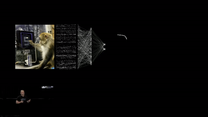
Neuralink’s latest public announcement featured a demonstration in which a monkey successfully controlled a computer cursor for the popular game of Pong using its brain.
The Fundamental Pipeline of this System can be Summarized as Follows:
Neuralink employs the N1 neural recording device to capture neural signals from the motor cortex of the subject during joystick interactions. This device is capable of recording from a large number of neural channels, providing rich spatiotemporal data for analysis.
- Neuralink employs the N1 neural recording device to capture neural signals from the motor cortex of the subject during joystick interactions. This device is capable of recording from a large number of neural channels, providing rich spatiotemporal data for analysis.
- Following this, a neural decoder is constructed using machine learning techniques to predict cursor velocity from patterns in the recorded neural activity. Specifically, the decoder maps neural signals to cursor movements through a linear or nonlinear transformation.
- Once the decoder is trained, the subject can use their cortical activity to directly control the cursor, bypassing the need for any physical movement.
In early 2021, around the time of Neuralink’s previous demonstration, the cursor control was reasonably accurate but slower than desired. Since then, the team has been dedicated to enhancing cursor speed and precision, as it forms the foundation of interacting with most computer applications.
The recent demonstration showcased significant improvements (~2x faster), with the cursor now being almost twice as fast. However, it still falls short of human capabilities, and the team is exploring innovative ways to improve it further.

While speed is essential, it’s also crucial to have a full range of functionalities. Most software applications have been developed for mouse and keyboard control over the decades, and it doesn’t make sense to overhaul the entire ecosystem for brain control, at least for now.
One of the most critical functionalities in computing is typing. In the demonstration below, Sake, a test monkey uses a virtual keyboard to type a message, similar to the one on a phone. The team achieved high speed and accuracy with the virtual keyboard, making typing fast and easy. However, typing on a virtual keyboard can be cumbersome and less efficient than using a physical keyboard.

To address the dire need of a better “typing” method, Neuralink has capitalized on some research from a group at Stanford in which they asked subjects to imagine handwriting letters, and then they decoded the letters from the subjects’ neural activity. (Willett et al.)
Inspired by this, the Neuralink team trained a monkey, to trace digits on an iPad to mimic handwriting. The team recorded Angela’s neural activity using the N1 device, but instead of decoding the cursor velocity, they decoded the digit being traced on the screen in real-time.
Although this approach ended up increasing typing rates, it required hundreds of examples and samples of each digit or character, making it unsuitable for scaling up to human use.

To overcome the challenge of scaling up the monkey’s ability to trace digits to human typing, Neuralink adopted an interaction-based approach. Rather than decoding digits directly, they first decode the hand trajectory of the user on the screen. Once they have decoded the hand trajectory, they can use any off-the-shelf handwriting classifier to predict the digits and characters being written. These classifiers can be trained on datasets such as the MNIST dataset.
The importance of this approach lies in the fact that they can now potentially decode any character in any language with only one neural decoder for hand trajectory. This means that users can write in English, Hebrew, Mandarin, or even monkey language, and the system can understand their intended message.
Zooming Out: BCI Readability| Plug-and-Play System
Challenge 1 | Firing Rate Variability:
In the field of BCIs, one of the challenges researchers face is the variability of the underlying signals they are trying to decode. In the real world, these signals are not static and can change significantly from day to day.
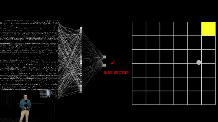
For example, one of the most commonly used signals for neural decoding is the firing rate of neurons in a particular area of the brain. However, this firing rate can vary widely over the course of just a few days, making it difficult to develop reliable decoding algorithms. In some cases, the average firing rate can change dramatically, even within a short span of time.

This presents a unique problem for Neuralink, as if they train their neural decoder on one day of data, and then try to use it on the next, the average firing rates can shift enough to cause a bias in the output of the model. As you can see below, this bias makes it hard for the cursor to move to the upper right corner, struggling to get there and moving more effortlessly in the opposite direction.
To tackle this issue, Neuralink is trying a variety of approaches to make their decoders more robust day to day.
- One such approach involves building models on large datasets of many days of data, enabling us to find patterns of neural activity that are stable across days.
- Another approach Neuralink is experimenting with is to continuously sample statistics of neural activity on the implant and use the latest estimates to pre-process the data before feeding it into the model.
Challenge 2 | Latency Between Neural Signals & Cursor Movement:
Another major challenges Neuralink faces is reducing the latency between the neural signal and the cursor movement on the screen. Any delay or inconsistency in this control loop can make it difficult for the user to control the cursor and result in overshoots, as can be seen in the example below.
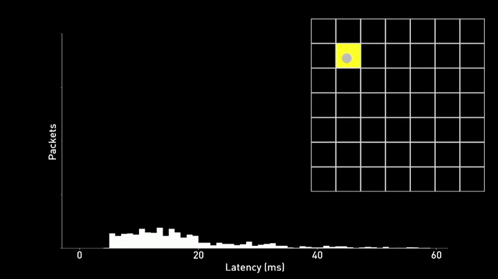
To address this problem, Neuralink has developed a new technique called phase lock. This method aligns the transmission of data packets from the implant to the exact moment when the Bluetooth radio is activated. By doing so, they reduce the time it takes for a neural spike to be incorporated into the prediction of their neural network. The result is a significant reduction in both the mean and variance of the latency distribution, which in turn makes it easier for the user to control the cursor.
Neuralink continues to work on mitigating issues related to the day-to-day variability of neural signals and minimizing the latency between the neural signal and cursor movement.
Zooming Out: Charging the N1 Chip
The N1 device is designed to operate continuously using a battery. When the battery runs low, it can be charged using wireless power transfer. However, unlike many consumer electronic devices, which can use a physical connector for charging, the N1 device faces several unique challenges due to being fully implantable.
- No Magnets For Alignment: Ensuring that the system can operate over a wide charging volume without relying on perfect alignment with magnets.
- Robustness to Disturbance: System must be robust to disturbance
- High Charging Rate: Complete charging quickly to avoid being overly burdensome
- Safety: When in contact with brain tissue, the outer surface of the implant must not rise by more than 2°C.
Therefore, designing a safe and effective charging mechanism for the N1 device requires careful consideration of these challenges.
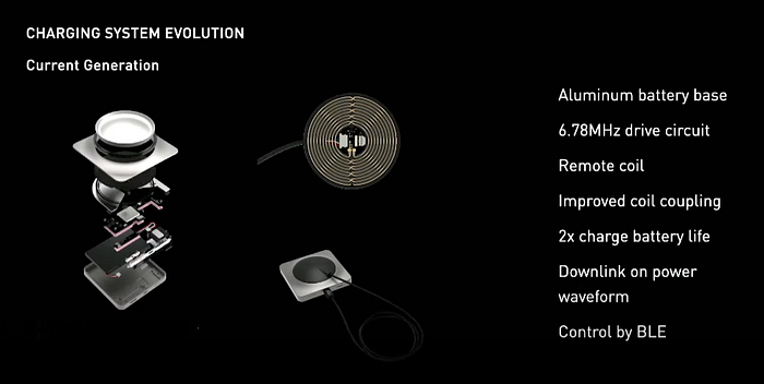
The charger currently used to charge Neuralink’s latest generation of implants is implemented in an aluminum battery base. This battery base contains the drive circuitry and includes a remote coil that is four times the size of their original device. This remote coil is also disconnectable, providing flexibility in charging.
One significant improvement of the current remote coil is its increased switching frequency, which improves the coil coupling. This production charger is already in use today, including several applications within Neuralink’s engineering and animal test facilities.
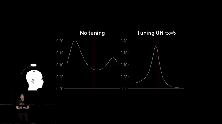
While high-quality factor coils exhibit good charging performance over relatively larger distances, bringing them closer to the implant causes a peak splitting effect. The best and highest-efficiency power transfer is pushed up into higher frequencies outside of the ISM band, which is required for compliance with regulated radiated emissions.
To address this issue in their next-generation charger, the team introduced dynamic tuning to adjust the resonant frequency of the transmit and receive coils in real-time. This enables them to change the properties of the coils just ahead of degraded performance, improving overall efficiency.
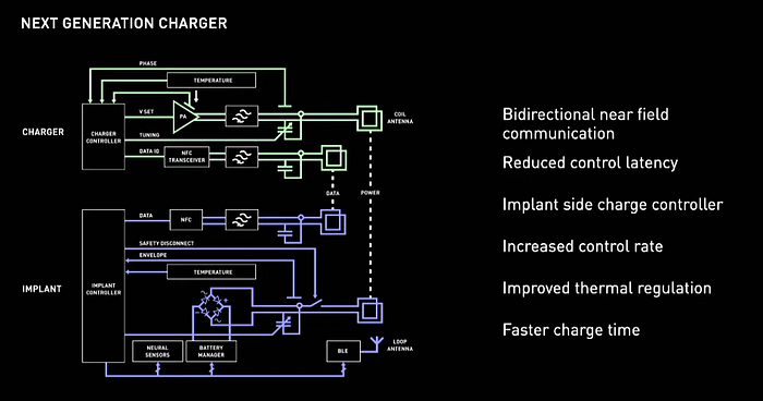
Currently, the electrical engineering team at Neuralink is developing a third-generation charger that includes bi-directional near-field communication. This has allowed them to reduce control latency and improve thermal regulation, resulting in faster charge times. Overall, these improvements demonstrate the team’s commitment to optimizing the performance of their implants and enhancing the user experience.
Zooming Out: N1 Chip Testing
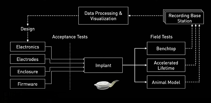
When Neuralink started building implants, they had a small manufacturing line, and data from an implant was manually collected by walking over with a laptop and connecting to it.
In order to achieve their goal of making an ultra-safe and ultra-reliable implant, they made several changes.
- Scaled up the manufacturing line and added a large suite of acceptance tests to test the functionality of each component and the final assembly
- Implants are then subjected to benchtop testing, accelerated lifetime, and animal models, and data is collected around the clock
- This data is processed by a series of cloud workers and displayed in an aggregate manner to empower engineers to answer any question about any implant at any time
Firmware Testing
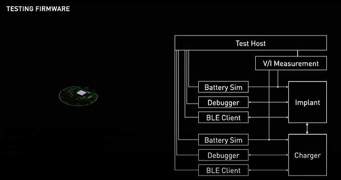
For firmware testing specifically, the implant contains a small microprocessor running firmware to manage its operations, and before a firmware update is released, it undergoes rigorous testing with both unit and hot around the loop tests, also known as hilltests.
To conduct a hill test, the battery, power rails, and microprocessor are instrumented, and each device is connected with a Bluetooth client and walked through various scenarios to test things like power consumption, real-time performance, security systems, and fault recovery mechanisms.

In the original implementation of the testing system, off-the-shelf components were used to start automating tests quickly, but these systems were constructed in a relatively austere fashion and were very difficult to maintain, making testing quickly become the bottleneck for development.
To alleviate this, the hardware and software teams developed a new system that integrates all the required components onto a single baseboard.
- The charger and implant hardware are on individual modules that plug into the baseboard, including one board with opposing coils to test charging performance.
- This architecture allows for rapid iteration of different hardware prototypes because they can be dropped into the system and reuse all the testing infrastructure
- The current and next generation ASICs can be hosted onto FPGAs and plug into the board as well, allowing a whole extra layer to be tested.
This system allows everything to be tested in one system from chip to cloud and has greatly accelerated the rate of development.
Implant Testing
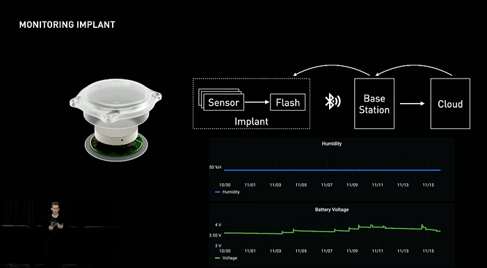
The implant captures its vital signs periodically and stores them in flash memory. When connected to a recording station, the implant streams this data off for analysis. This allows the team to get insights into the integrity of the implant’s enclosure and battery health.
The system is designed to provide continuous, automated monitoring without any intervention, giving the team 24/7 visibility into the quality of every device. In addition, the system can provide high-fidelity information on demand to investigate different atypical situations.
This monitoring system is an essential part of the team’s efforts to create an ultra-safe and ultra-reliable implant. By collecting data around the clock, they can identify any issues early on and take proactive steps to address them. This information is also fed back into the design process to inform future iterations of the implant. Overall, this system helps the team to ensure that every implant they produce is of the highest quality and meets the highest standards of safety and reliability.
Electrode Testing
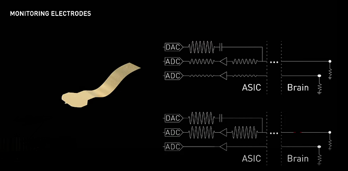
To capture good quality neural signals, the electrodes must have low impedance, which is a measure of the resistance to the flow of electrical current. To monitor impedance, Neuralink has dedicated circuitry on the neural sensor, which uses an onboard DAC to play a test tone on a single channel while simultaneously recording the response signal on both that channel and physically adjacent channels using their ADCs.
This allows them to measure the impedance of every channel and map different physical phenomena to different characteristic signatures. For example, an open channel will appear as a very large response on the channel, while shorter channels will appear as a large response on neighboring channels.
By analyzing the purity of the signal coming back, they can also validate that the analog front end of the neural sensor is operational. In Neuralink’s original implementation of doing these impedance scans, it took four hours to get through all 1000 channels. However, they have since optimized the process by paralyzing the tests, downsampling and filtering, and moving much of the calculation to the firmware side. As a result, they can now scan all 1000 channels in just 20 seconds, which means they can run impedance tests on every implant every day.
Their internal dashboards play back a history of this impedance data, which provides them with a quantitative insight into the interface between biology and electronics. This allows them to ensure that they are capturing good quality neural signals and maintaining the integrity of the electrodes. By doing so, they can continue to develop ultra-safe and ultra-reliable implants.
Accelerated Lifetime Testing System
Neuralink has made significant strides in developing a system that enables accelerated lifetime testing of their implant devices, which is a critical step in improving their product quality and reliability.

By mimicking the internal chemistry of tissue and aggressively cycling the internal electronics of the implant, Neuralink has achieved a conservative 4X acceleration factor, significantly reducing the time required to test the device’s failure modes at scale.
Another significant challenge Neuralink faces is preventing moisture ingress into their implant devices, which can lead to electronic failures. To address this challenge, they have developed an internal humidity sensing system that is highly sensitive and can detect even small and slow humidity rises from diffusion through implant materials. They have also used this system to track internal humidity data from implants in some of their animals for over a year, providing valuable insights into the long-term performance of their devices.
By continuously monitoring internal humidity levels and using their accelerated lifetime testing system, Neuralink can identify potential issues and make improvements to their implant devices before they are implanted into humans. This proactive approach to quality control will not only increase the reliability of their product but also reduce the need for animal testing, which aligns with their commitment to ethical and sustainable practices.
Gaps in N1 Testing
As they continue to push the boundaries of implant technology, there are a multitude of exciting challenges that lie ahead. These challenges include:
- Introducing mechanical stressing
- Mimicking brain proxy micro motion
- Replicating tissue growth around the threads for more comprehensive and representative accelerated testing
By tackling these challenges head-on, Neuralink can ensure that their implant technology is not only cutting-edge, but also thoroughly tested and reliable.
Zooming Out: N1’s Surgery Engineering
N1 Surgical Process of Implantation
- Targeting: The first step is to locate the target area in the brain where the implant needs to be placed.
- Incision: Once the target area is identified, an incision is made in the skin overlying the skull.
- Craniectomy: A small section of the skull is then drilled out using specialized surgical tools to create a hole for the implant.
- Removal of Dura: The tough outer layer of the meninges, called the dura, is removed to expose the brain tissue underneath.
- Insertion of Electrodes: Thin and flexible threads of electrodes are then carefully inserted into the brain tissue through the hole in the skull. The electrodes are designed to pick up electrical signals from individual neurons or groups of neurons.
- Placement of Implant: The N1 device, which contains the necessary electronics for recording and transmitting the neural signals, is placed into the hole created in the skull.
The neural implant device incorporates a robotic system to perform the thread insertion aspect of the surgery, a task that would be challenging for a human to do manually. Inserting 64 tiny threads with precise depth and position into a Jello-like substance covered by Saran Wrap within a reasonable amount of time would be an overwhelming challenge for any neurosurgeon.
This is where R1, the surgical robot, comes in to perform this crucial step, while the neurosurgeon handles the remaining parts of the surgery.
The team recognizes that there is a need to optimize the procedure further to enable one neurosurgeon to oversee multiple procedures simultaneously, thus making the procedure even more accessible and affordable.
Overcoming the challenges encountered in optimizing the robot’s thread insertions has required the team to focus on improving the mechanical packaging and ensuring that there is precise imaging and illumination.
By combining several optical paths into one, the robot can perform vessel avoidance in real-time, which significantly enhances the safety and accuracy of the procedure.
Next Generation Development Process
To ensure that Neuralink’s new technology remains accessible for early adopters, they must find a solution that makes device upgrades or replacements as easy as the initial installation.
However, this is a challenging problem for many medical device companies, as the body’s healing response makes it difficult to remove and replace devices that have been encapsulated by tissue over time. Despite this challenge, significant progress has been made towards enabling device upgrades and replacements, which we will discuss today.

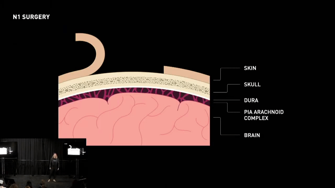
Before delving into the challenges of device upgrades, let’s first understand the anatomy. Under the skin, there is the skull, followed by the dura, a tough membrane that separates the bone from the brain.
Between the dura and the brain, there is the pia-arachnoid complex, a fluid-filled suspension that protects and supports the brain. When installing a device, the surgeon removes a disc of skull and dura to expose the brain surface, and the device is then placed to replace the removed material.
The challenge with device upgrades arises at this interface because over time, any empty volume created by the removal of the device is filled with tissue that encapsulates the device and its threads. This tissue layer makes the removal of the device challenging, as the threads of the device would slip right out of the brain if removed.
To address this challenge, the company has built tools in-house to study this response and characterize it. Using histology and micro CT, they have identified a layer of tissue that has formed above the surface, encapsulating the threads and adhering to the surrounding tissue. The company has explored various avenues for designing around this sealing process and finding a solution to make device upgrades seamless.

Their best successes have come from making the procedure less invasive. Instead of directly exposing the brain’s surface, they keep the dura in place, maintaining the body’s natural protective barrier. This prevents encapsulation of the brain’s surface, which makes the surgery simpler and safer.
However, this approach doesn’t come without its challenges. The dura is a tough, opaque membrane composed of a dense network of collagen fibers, as seen in the SEM images provided. This presents an array of technical challenges for inserting the company’s electrodes. One of these challenges is imaging through the dura.

The current custom optical systems offer incredible capabilities for imaging the exposed brain surface, but once the dura is in place, the dense vasculature at the brain surface cannot be seen due to the attenuation caused by the dura. To solve this problem, the company is developing a new optical system that uses medical standard fluorescent dye to image vessels underneath the tissue. This system highlights vessels by perfusing dye through them, allowing the company to target and avoid blood vessels underneath the dura.
The company is also exploring applying their laser imaging system to deeper tissue structures. In the image below, a section of the tissue layers underneath the dura is shown, compiled from multiple volumes from the company’s optical coherence demography system. The future goal is for these new systems, when combined with correlation to pre-op imaging such as MRI, to enable precise targeting without directly exposing the brain surface.

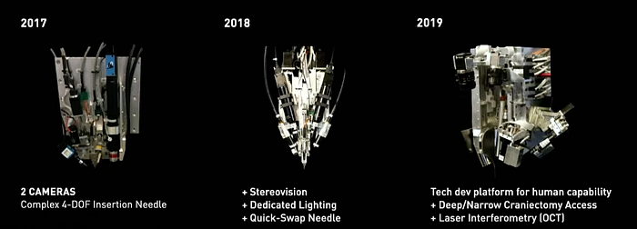
Needle Design & Manufacturing
As discussed, the dura, a tough layer that surrounds the brain, is a good protector of the brain. However, it poses challenges when trying to insert threads into it. The dura can be over a millimeter thick, which is relatively large compared to the 40-micron needles used for insertion. Imagine scaling up the needle to the size of a pencil, this would result in the dura being over four inches thick.

The brain is soft underneath the tough dura, so the needle must be sharp enough to puncture it. Otherwise, it would just keep dimpling the surface. Another challenge is that the thread must also be inserted along with the needle. Therefore, optimizing the combined profile of the needle and thread is necessary.
The process of making the needle involves starting with a length of 40-micron wire made out of tungsten and alloyed with a little bit of rhenium for added ductility. The features of the needle and cannula are cut using a femtosecond laser with sub-micron precision. The laser cutting process has been optimized, resulting in the time taken to make a needle being reduced from 22 minutes to 6 minutes, with a yield increase from 58% to 91%.

Iterating on designs is crucial, and the femtosecond laser ablation workflow allows for several iterations per day. The latest design can insert through nine layers of dura, totalling three millimeters, on a bench top, which is far more than we could ever expect in a human.
To iterate on different threads, the team has an in-house microfabrication process. With a newly rebuilt clean room, they can iterate on new designs in just a matter of days. Testing is also an essential part of the process, as it is necessary to ensure that the new designs work effectively.
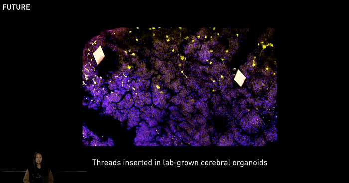
Proxy Design
When we implant medical devices and threads into the human body, they are subjected to a complex biological environment. However, learning directly from biology can be slow, so Neuralink engineers are developing synthetic materials that mimic the biological environment. This approach allows them to learn as much as possible on the benchtop and move away from the industry standard of animal testing.
However, developing accurate proxies that replicate the implant environment is challenging. The implant environment is composed of multiple anatomical layers, each with unique properties. As time passes, new tissue forms at the implant site, filling any available space. Furthermore, motion related to cardiovascular activity and head movement adds to the complexity.
To address these challenges, researchers at Neuralink are engineering materials using feedback from biology. This involves mechanical characterization of tissue and analysis of interactions at the thread-tissue interfaces. During surgery, they use custom hardware and software that modifies their surgical robot to double up as a sensitive characterization tool. They then use the data collected to optimize their materials so that they behave mechanically, chemically, and structurally just like biology.
The researchers have come a long way from their first brain proxy, which consisted of agar and a pyrofoam sheet sitting on a plate. Today, they have upgraded to a composite hydrogel-based brain proxy that better mimics the modulus of the real human brain. They have also incorporated a duraproxy and developed an injectable soft tissue proxy that has allowed them to perform benchtop mock explant testing.
In the future, researchers hope to create a variety of proxies, including a surgery proxy with integrated soft tissue, brain, bone, skin, or even a whole body. They also hope to develop a brain proxy that simulates motion, vasculature, and electrophysiological activity and a biological proxy to test biocompatibility and electrical stimulation. Ongoing work, including lab-grown cerebral organoids, will help researchers get closer to their proxy of the future.
We want to talk to you!
Mikael Haji →
📫 email: mikaelhaji@gmail.com
🕴 linkedin: @mikaelhaji
Anush Mutyala →
📫 email: mutyalaanush@gmail.com
🕴 linkedin: @anushmutyala